- 您现在的位置:买卖IC网 > Sheet目录1212 > DS1780K (Maxim Integrated Products)KIT EVALUATION DS1780
�� �
�
�DS1780�
�The� worse� such� accident� would� be� connecting� -12V� to� +12V;� a� total� of� 24V� difference,� with� the� series�
�resistors� this� would� draw� a� maximum� of� approximately� 24� ma.�
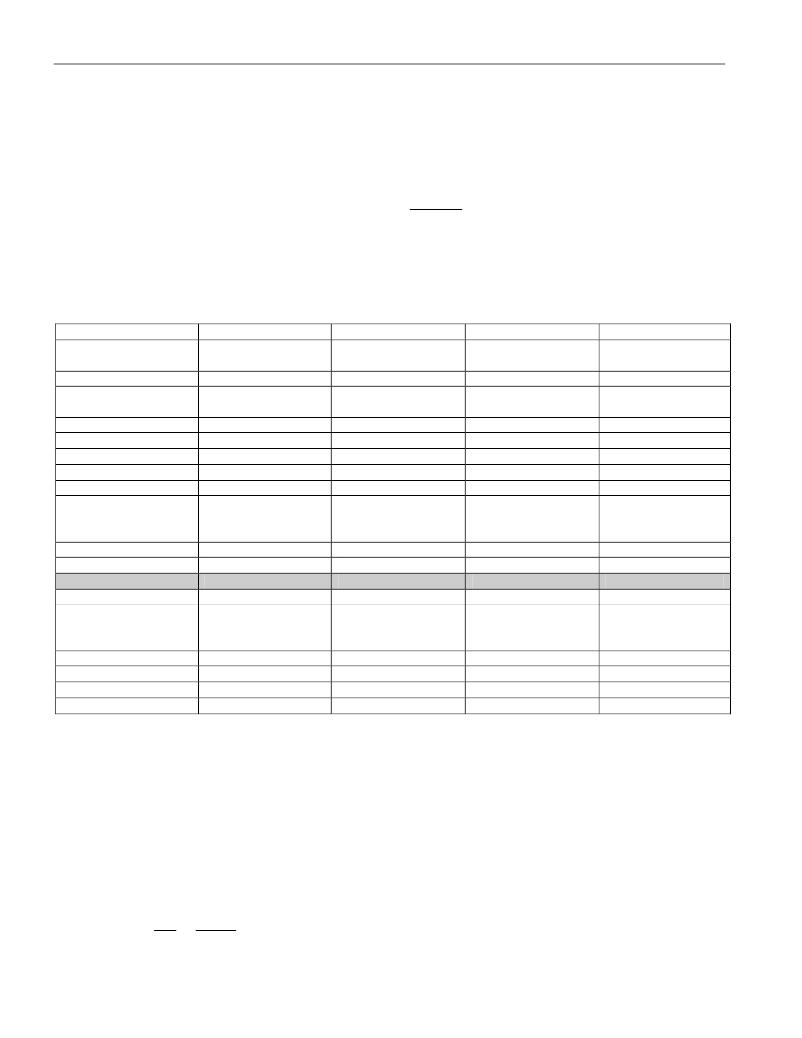
�The� internal� scaling� factor� depends� upon� the� particular� input.� The� +12V� IN� ,� +5V� IN� ,� +3.3V� IN� ,� and� +2.5V� IN�
�inputs� are� internally� scaled� such� that� the� nominal� value� of� the� respective� supply� corresponds� to� 3/4� of� full�
�range,� or� a� decimal� count� of� 192.� The� approximate� resolution� is� thus� equal� to:�
�LSb� (V� NOM� )� @�
�4/3 V� NOM�
�256�
�This� is� depicted� below� in� Table� 5.�
�VOLTAGE/DATA� RELATIONSHIPS� FOR� POSITIVE� ONLY� VOLTAGE� INPUTS�
�(+12V� IN� ,� +5V� IN� ,� +3.3V� IN� ,� and� +2.5V� IN� )� Table� 5�
�INPUT� PIN� +12V� IN� +5V� IN�
�LSb� WEIGHTING� 62.5� 26.0�
�(mV)�
�+3.3V� IN�
�17.2�
�+2.5V� IN�
�13.0�
�ADC� RESULT� (BASE�
�PIN� VOLTAGE� (V)�
�PIN� VOLTAGE� (V)�
�PIN� VOLTAGE� (V)�
�PIN� VOLTAGE� (V)�
�10)�
�0�
�1�
�2�
�3�
�4�
�?�
�?�
�?�
�190�
�191�
�192�
�193�
�?�
�?�
�?�
�252�
�253�
�254�
�255�
�0�
�0.063�
�0.125�
�0.188�
�0.25�
�?�
�?�
�?�
�11.875�
�11.938�
�12.0�
�12.063�
�?�
�?�
�?�
�15.75�
�15.813�
�15.875�
�15.938�
�0�
�0.026�
�0.052�
�0.078�
�0.104�
�?�
�?�
�?�
�4.948�
�4.974�
�5.0�
�5.026�
�?�
�?�
�?�
�6.563�
�6.589�
�6.615�
�6.641�
�0�
�0.017�
�0.034�
�0.052�
�0.069�
�?�
�?�
�?�
�3.266�
�3.283�
�3.3�
�3.317�
�?�
�?�
�?�
�4.331�
�4.348�
�4.366�
�4.383�
�0�
�0.013�
�0.026�
�0.039�
�0.052�
�?�
�?�
�?�
�2.474�
�2.487�
�2.5�
�2.513�
�?�
�?�
�?�
�3.281�
�3.294�
�3.307�
�3.32�
�The� other� two� voltage� inputs� use� a� slightly� different� scaling� technique,� due� to� the� nature� of� the� PC� voltage�
�they� are� monitoring.� Because� processor� voltage� (V� CCP� )� can� vary� to� 3.6V,� the� +V� CCP1� and� +2.5V� S� /+V� CCP1�
�inputs� are� internally� scaled� such� that� the� ADC� result� is� 0h� for� a� 0V� input� and� the� maximum� value� of� FFh�
�is� returned� for� a� voltage� of� 3.60V.� This� corresponds� to� an� LSb� weighting� of� 14.1� mV.�
�The� inputs� can� also� be� used� to� monitor� a� negative� supply,� such� as� -12V.� However,� a� resistor� ladder� and�
�positive� reference� voltage� (V� REF� )� must� be� used� (see� Figure� 1)� such� that� input� voltage� to� the� DS1780�
�swings� between� OV� and� +3.6V.� Assuming� the� DS1780� +V� CCP1� and� +2.5V� S� /+V� CCP2� pins� have� infinite�
�input� impedance� and� the� V� REF� is� a� perfect� supply,� then� the� resolution� and� range� of� -12V� input� are:�
�ê� ú�
�?�
�?�
�LSb� (R� 1� ,� R� 2� )� @�
�3.6�
�255�
�é� R� 1� +� R� 2� ù�
�R� 1�
�9� of� 28�
�发布紧急采购,3分钟左右您将得到回复。
相关PDF资料
DS1863K
KIT EVAL FOR DS1863
DS1864K
KIT EVAL FOR DS1864
DS21349DK
KIT DESIGN FOR DS21349
DS21352DK
KIT DESIGN FOR DS21352
DS21354DK
KIT DESIGN FOR DS21354
DS21458DK
KIT DESIGN FOR G511DS21458
DS2156DK
KIT DESIGN FOR DS2156
DS21Q348DK
KIT DESIGN FOR DS21Q348
相关代理商/技术参数
DS17885
制造商:DALLAS 制造商全称:Dallas Semiconductor 功能描述:3V/5V Real-Time Clock
DS17885-3
功能描述:实时时钟 RoHS:否 制造商:Microchip Technology 功能:Clock, Calendar. Alarm RTC 总线接口:I2C 日期格式:DW:DM:M:Y 时间格式:HH:MM:SS RTC 存储容量:64 B 电源电压-最大:5.5 V 电源电压-最小:1.8 V 最大工作温度:+ 85 C 最小工作温度: 安装风格:Through Hole 封装 / 箱体:PDIP-8 封装:Tube
DS17885-3+
功能描述:实时时钟 3V/5V RTC RoHS:否 制造商:Microchip Technology 功能:Clock, Calendar. Alarm RTC 总线接口:I2C 日期格式:DW:DM:M:Y 时间格式:HH:MM:SS RTC 存储容量:64 B 电源电压-最大:5.5 V 电源电压-最小:1.8 V 最大工作温度:+ 85 C 最小工作温度: 安装风格:Through Hole 封装 / 箱体:PDIP-8 封装:Tube
DS17885-5
功能描述:实时时钟 RoHS:否 制造商:Microchip Technology 功能:Clock, Calendar. Alarm RTC 总线接口:I2C 日期格式:DW:DM:M:Y 时间格式:HH:MM:SS RTC 存储容量:64 B 电源电压-最大:5.5 V 电源电压-最小:1.8 V 最大工作温度:+ 85 C 最小工作温度: 安装风格:Through Hole 封装 / 箱体:PDIP-8 封装:Tube
DS17885-5+
功能描述:实时时钟 3V/5V RTC RoHS:否 制造商:Microchip Technology 功能:Clock, Calendar. Alarm RTC 总线接口:I2C 日期格式:DW:DM:M:Y 时间格式:HH:MM:SS RTC 存储容量:64 B 电源电压-最大:5.5 V 电源电压-最小:1.8 V 最大工作温度:+ 85 C 最小工作温度: 安装风格:Through Hole 封装 / 箱体:PDIP-8 封装:Tube
DS17885-DS17887
制造商:DALLAS 制造商全称:Dallas Semiconductor 功能描述:3V/5V Real-Time Clock
DS17885E3
制造商:MAXIM 制造商全称:Maxim Integrated Products 功能描述:Real-Time Clocks
DS17885E-3
功能描述:实时时钟 3V/5V RTC RoHS:否 制造商:Microchip Technology 功能:Clock, Calendar. Alarm RTC 总线接口:I2C 日期格式:DW:DM:M:Y 时间格式:HH:MM:SS RTC 存储容量:64 B 电源电压-最大:5.5 V 电源电压-最小:1.8 V 最大工作温度:+ 85 C 最小工作温度: 安装风格:Through Hole 封装 / 箱体:PDIP-8 封装:Tube